Saturday, August 21, 2010

Anti Theft Car wireless alarm

This is anti theft alarm with wireless connectivity ,called Anti Theft Car wireless alarm The FM radio-controlled anti- theft alarm can be used with any vehicle having 6- to 12-volt DC supply system. The mini VHF, FM transmitter is fitted in the vehicle at night when it is parked in the car porch or car park. The receiver unit with CXA1019,
Anti Theft Car wireless alarm
a single IC-based FM radio module, which is freely available in the market at reasonable rate, is kept inside. Receiver is tuned to the transmitter's frequency. When the transmitter is on and the signals are being received by FM radio receiver, no hissing noise is available at the output of receiver. Thus transistor T2 (BC548) does not conduct. This results in the relay driver transistor T3 getting its forward base bias via 10k resistor R5 and the relay gets energised. When an intruder tries to drive the car and takes it a few metres away from the car porch, the radio link between the car (transmitter) and alarm (receiver) is broken. As a result FM radio module gene-rates hissing noise. Hissing AC signals are coupled to relay switching circ- uit via audio transformer. These AC signals are rectified and filtered by diode D1 and capacitor C8, and the resulting positive DC voltage provides a forward bias to transistor T2. Thus transistor T2 conducts, and it pulls the base of relay driver transistor T3 to ground level. The relay thus gets de-activated and the alarm connected via N/C contacts of relay is switched on. If, by chance, the intruder finds out about the wireless alarm and disconnects the transmitter from battery, still remote alarm remains activated because in the absence of signal, the receiver continues to produce hissing noise at its output. So the burglar alarm is fool-proof and highly reliable.

Game Show Timers Schema electronic Circuit


Many people have expressed an interest in the game show timer from the "end user" viewpoint instead of the "hobbyist" viewpoint. These interested folks don't have much electronic assembly experience but they are highly motivated and are willing to give it a try in order to get the end result. It is with these people in mind that the following circuit was developed. This is my favorite and the one I recommend.

Here is a really simple game show timer designed with the beginner in mind! The power source is an ordinary 12 volt lantern battery or battery pack made up of C or D cells. The lamps may be ordinary flashlight bulbs; the prototype uses 750 mA Krypton types (KPR112) with wires soldered directly onto the bulbs. The control devices may be just about any non-sensitive gate SCRs or triacs with a current rating of a few amps. Avoid SCRs that trigger with 100s of microamperes; you want a gate trigger current of a few mA or else you will have trouble with more than one light coming on at once. A low value resistor, perhaps 470 ohms may be added from gate to -12 volts to reduce false triggering.

SCRs are shown and triacs may be substituted by connecting MT1 to the negative battery terminal and MT2 to the lamps. In fact, the two types of devices could probably be mixed if that is what the junk box has to offer! (But not sensitive gate types!) The zener is an ordinary 9 volt, 1 watt type like the 1N4739. The 100 ohm resistor may be any type with a rating of 1/8 watt or more. The reset/power button is an ordinary toggle switch and the pushbuttons are any convenient normally-open type

Electronic Circuit Symbols Components


Circuit diagrams appearance how cyberbanking apparatus are affiliated together. Anniversary basic is represented by a attribute and a few are apparent here, for added symbols amuse see the Ambit Symbols page.

Circuit diagrams and basic layouts

Circuit diagrams appearance the access as acutely as accessible with all affairs fatigued neatly as beeline lines. The absolute blueprint of the apparatus is usually absolutely altered from the ambit diagram and this can be ambagious for the beginner. The abstruse is to apply on the connections, not the absolute positions of components.

The ambit diagram and stripboard blueprint for the Adjustable Timer activity are apparent actuality so you can see the difference.


A ambit diagram is advantageous back testing a ambit and for compassionate how it works. This is why the instructions for projects accommodate a ambit diagram as able-bodied as the stripboard or printed ambit lath blueprint which you charge to body the circuit.

Drawing ambit diagrams

Drawing ambit diagrams is not difficult but it takes a little convenance to draw neat, bright diagrams. This is a advantageous accomplishment for science as able-bodied as for electronics. You will absolutely charge to draw ambit diagrams if you architecture your own circuits.

Follow these tips for best results:

Make abiding you use the actual attribute for anniversary component.

Draw abutting affairs as beeline curve (use a ruler).

Put a 'blob' () at anniversary alliance amid wires.

Label apparatus such as resistors and capacitors with their values.

The absolute (+) accumulation should be at the top and the abrogating (-) accumulation at the bottom. The abrogating accumulation is usually labelled 0V, aught volts.

If you are cartoon the ambit diagram for science amuse see the area about cartoon diagrams the 'electronics way'.

If the ambit is complex:

Try to align the diagram so that signals breeze from larboard to right: inputs and controls should be on the left, outputs on the right.

You may omit the array or ability accumulation symbols, but you charge accommodate (and label) the accumulation curve at the top and bottom.

Drawing ambit diagrams the 'electronics way'

Circuit diagrams for electronics are fatigued with the absolute (+) accumulation at the top and the abrogating (-) accumulation at the bottom. This can be accessible in compassionate the operation of the ambit because the voltage decreases as you move bottomward the ambit diagram.

Circuit diagrams for science are commonly fatigued with the array or ability accumulation at the top. This is not wrong, but there is usually no advantage in cartoon them this way and I anticipate it is beneath accessible for compassionate the circuit.

I advance that you consistently draw your ambit diagrams the 'electronics way', alike for science!

[I achievement your science abecedary won't apperception too much!]

Note that the abrogating accumulation is usually alleged 0V (zero volts).

This is explained on the Voltage and Current page.

Dome light dimmer With delay for Cars

Intro & abnegation

For all you guys out there that appetite a crumbling arch ablaze (aka address ablaze aka theatre lighting) after accepting to pay for one, you can body your own. I accept absorbed the schematics and you can body it for a few bucks accustomed that you don't accept any additional apparatus lying about contrarily it can amount you absolutely nothing. Of advance you can rip some genitalia from your TV, CD player, radio, etc., but I'm not amenable for the accident you account this way

The way it works

I won't bother you with abstruse details, but if addition is absorbed aloof let me apperceive and I'll explain in detail. For now aloof the basics. There are two stages: aboriginal one is dabbling and the additional one is fading. Back you accessible the aperture the ablaze turns on. You get central and abutting the door, but the ablaze stays on (delay stage) for an adjustable aeon of time (0-40 sec. for the ethics in the scheme, but you can calmly adapt that i.e. put a bigger capacitor) so you can see area to admit the key or do whatever you do back you get in the car, again fades abroad (fading stage) with an adjustable speed. If you affix the ACC wire (which is absolutely optional) back you about-face the key to ACC position the ablaze turns off (actually fades) alike if the dabbling date is not over (it cancels the adjournment stage).

Setup

The SR1 trimmer pot adjusts the dabbling time (the aeon that the ball is at abounding intensity) and you accept a "witness" LED that is lit during the dabbling stage; that way you can set it visually to whatever continuance you like. Back the aboriginal date ends (marked by the LED not actuality lit anymore) enters the additional date - fading. The SR2 trimmer pot adjusts the crumbling time (or acceleration if you prefer)

The angel aloft depicts how the arch ablaze about-face is usually affiliated (depending on the accomplish and archetypal of your car the affiliation may be altered in which case you'll accept to amount it out).

The angel beneath shows the schematic and the access to the arch ablaze switch.
Dome light dimmer (with delay)

Dome light dimmer (with delay) schema

Wiper Speed Control Circuits

A continuously alive wiper in a car may prove to be a nuisance, abnormally back it is not aqueous heavily. By application the ambit declared actuality one can alter across-the-board amount of the wiper from already a additional to already in ten seconds. The ambit comprises two timer NE555 ICs, one CD4017 decade counter, one TIP32 disciplinarian transistor, a 2N3055 ability transistor (or TIP3055) and a few added detached components. Timer IC1 is configured as a mono- abiding multivibrator which produces a beating back one presses
about-face S1 momentarily. This beating acts as a alarm beating for the decade adverse (IC2) which advances by one calculation on anniversary alternating alarm beating or the advance of about-face S1. Ten presets (VR1 through VR10), set for altered ethics by balloon and error, are acclimated at the ten outputs of IC2. But back alone one achievement of IC2 is aerial at a time, alone one preset (at called output) finer comes in alternation with timing resistors R4 and R5 affiliated in the ambit of timer IC3 which functions in astable mode. As presets VR1 through VR10 are set for altered values, altered time periods (or frequencies) for astable multivibrator IC3 can be selected. The achievement of IC3 is activated to pnp disciplinarian transistor T1 (TIP32) for active the final ability transistor T2 (2N3055) which in about-face drives the wiper motor at the called ambit speed. The ability accumulation for the wiper motor as able-bodied as the ambit is broke from the vehicle�s array itself. The continuance of monostable multivibrator IC1 is set for a about one additional period.

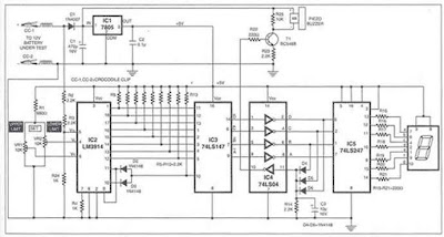
Charge Monitor For 12V Lead Acid Battery


A array is a basic aspect of any battery-backed system. In abounding cases the array is added big-ticket than the arrangement it is abetment up. Hence we allegation to accept all activated measures to conserve array life.

As per manufacturer's abstracts sheets, a 12V rechargeable lead-acid array should be operated aural 10. IV and 13.8V. Back the array accuse college than 13.8V it is said to be overcharged, and back it discharges beneath 10.IV it can be acutely discharged. A distinct accident of blackmail or abysmal acquittal can accompany bottomward the charge-holding accommodation of a array by 15 to 20 per cent.

It is accordingly all-important for all anxious to adviser the allegation akin of their batteries continuously. But, in practice, abounding of the array users are clumsy to do so because of non-avail�ability of reasonably-priced ecology equipment. The ambit abstraction presented actuality will ample this abandoned by accouterment a ambit for ecology the allegation akin of lead-acid batteries continuously. The ambit possesses two basic features:

First, it reduces the claim of animal absorption by about 85 per cent.

Second, it is a awful authentic and adult method.

Input from the array beneath analysis is activated to LM3914 1C. This activated voltage is ranked anywhere amid 0 and 10, depending aloft its magnitude. The lower advertence voltage of 10.IV is ranked '0' and the high voltage of 13.8V is ranked as '10.' (Outputs 9 and 10 are logically ORed in this circuit.) This arrangement of advertence voltages is explained later.

1C 74LS147 is a decimal-to-BCD antecedence encoder which converts the achievement of LM3914 into its BCD complement. The accurate BCD is acquired by application the hex inverter 74LS04. This BCD achievement is displayed as a decimal chiffre afterwards con�version application IC5 (74LS247), which is a BCD-to-seven-segment decoder/driver. The seven-segment LED affectation (LTS-542) is acclimated because it is accessible to apprehend compared to a bar blueprint or, for that matter, an alternation meter. The allegation cachet of the array can be bound affected from the display. For instance, if the affectation shows 4, it agency that the array is answerable to 40 per cent of its best amount of 13.8V.

The use of agenda attempt enables us to apply a buzzer that sounds whenever there is an blackmail or abysmal discharge, or there is a allegation to conserve array charge. A buzzer is active in the ambit such that it sounds whenever battery-charge avalanche to ten per cent. At this point it is recommended that accidental amount be switched off and the actual allegation be conserved for added important purposes.

Another simple combinational argumentation ambit can additionally be advised that will complete the buzzer back the affectation shows 9. Further charging should be chock-full at this point in adjustment to pre�vent overcharge.

The ambit is powered by the array beneath test, via a voltage regulator 1C. The ambit takes about 100 mA for its operation.

For calibrating the high and lower advertence levels, a agenda multimeter and a capricious adapted ability accumulation antecedent are required. For calibrating the lower advertence voltage, chase the accomplish accustomed below:

Set the achievement of ability accumulation antecedent to 10. IV.

Connect the ability accumulation antecedent in abode of the battery.

Now the affectation will appearance some reading. At this point alter preset VR2 until the account on the affectation aloof changes from 1 to 0.

The college advertence voltage is calibrated analogously by ambience the ability accumulation to 13.8V and capricious preset VR1 until account on the affectation aloof changes from 8 to 9
Charge Monitor For 12V
Charge Monitor For 12V Lead Acid Battery Diagram

RF Transceiver Module - High Frequency RF Transceiver - 900 Mhz

RF Transceiver Module - High Frequency RF Transceiver - 2.4GHz. Transceiver

RF Modules - RF Transceiver

Laipac offers several low cost RF modules for high speed data transmission. Low cost modules include the TLP/RLP series of transmitters and receivers . These modules are very versatile, therefore perfect for OEM customers. We also offer a variety of Transceivers for voice, data & voice and data & voice & video. The transceivers are great for more complex, full duplex telemetry or communications.

RF Transceiver Module

Model

Main Features

Frequency

Voltage

Data Rate

Sensitivity

Max. Consumption

RF900DV

16 Channels

902.525~
904.625MHZ. & 902.525 ~

5V (Base) &
3.6V (Remote),

200Kbps~28.8Kbps

-103dB

80mA

TRF-2.4G High Speed Data/Transceiver 2.4Ghz Frequency : 2.4~2.524 GHz 3V Estimated 100mts @250Kbps ; 50mts @1Mbps, Line of Sight -90dB @250kbps
-80dB @1000kbps 18 mA@250kbps

WIRELESS USB DONGLE - AWP24U


Artaflex Inc 2.4GHz Rf Transceiver Module AMR, HID, RKE, Smart Appliances AWP24U

WIRELESS USB DONGLE - AWP24U - RF and RFID
Digi-Key Part Number 748-1002-ND
Price Break Unit Price Extended Price
1 31.99000 31.99
10 24.99000 249.90
100 19.99000 1999.00
500 17.75004 8875.02
1000 16.99001 16990.01
Manufacturer Part Number AWP24U
Description WIRELESS USB DONGLE
Quantity Available 12
All prices are in US dollars.

Wireless USB - RF Transceivers™

Cypress's WirelessUSB(TM) solutions are designed for short-range, multipoint-to-point connectivity. WirelessUSB enables PC Human Interface Device (HID) peripherals, such as wireless mice, keyboards, media-center remote controls and presenter tools, wire replacement with a low-power and highly reliable, 2.4GHz wireless solution. Cypress's patented WirelessUSB technology offers unparalleled feature set to enable superior RF performance, interference immunity, and maximum battery life.

To further extend the flexibility and programmablity of Cypress's Wireles portfolio, PRoC(TM) - Programmable Radio-system on-a Chip - integrates a flexible 8-bit microcontroller with the 2.4GHz radio transceiver in a single chip solution. The PRoC solutions offers a unique capability of component integration to enable extremely small form factor designs for low-power wireless systems.

Furthermore, Cypress's easy-to-use Wireless hardware and software tools reduce wireless complexity for customers, significantly reducing design cycles, from end-to-end wireless keyboard and mouse reference designs to production ready, pre-certified RF modules. Modules provide complete drop-in solutions, including the complete (silicon and all external components) printed circuit board (PCB) to meet maximum performance requirements. Cypress has partnerships with Ontario-based Artaflex, Fremont, CA-based Unigen, and Italy-based Aurel to offer a wide portfolio of wireless modules. Information and datasheets for these modules can be found on their websites:


Company NameCompany DescriptionDetailed Info on CYPros
Artaflex Inc.Artaflex (Formerly Baranti) is an award-winning electronic design and manufacturing services company, serving major OEMs across the United States and Canada. Artaflex designs electronic products and modules for clients ranging from technology startups to Fortune 500 companies. The company has particular expertise in digital video / imaging products, but maintains a diverse design portfolio in multimedia, consumer electronics, portable embedded products, health care, industrial controls, and computing.Artaflex Inc.
Aurel

AUREL was established in the 1970 with the mission to develop and promote thick film technology and equipments.

AUREL products include: thick film hybrid with custom design and assemblies, proprietary design radio frequency modules, avionic application modules, electromedical instruments, remote controls.

AUREL offers advanced technological solutions and manufacturing processes which continuously guarantee the requested high level of quality.

AUREL facilities extended over 4.000 SM with more than 100 skilled workers plus an International sales network

AUREL, leader into Short Range Devices & Radiofrequency modules is ISO 9001 Ed. 2000 for full design and manufacturing process.

Not part of CYPros program yet. Please contactAureldirectly.
Unigen Corp.Unigen is a leader in the design and manufacture of OEM memory, DC-DC power conversion, wired and wireless communication, flash memory, and other standard and customer specific module solutions. Unigen supplies silicon, modules, and services to leading clients in the PC, server, networking, telecommunication, imaging, medical, defense, and mobile computing industries. Unigen's core competency is the design and manufacture of precise and complex standard and customer module products. Unigen services includes contract manufacturing and assembly, worldwide product distribution, supply chain management, testing, prototyping, product assurance, and post sales support. Unigen is headquartered in Fremont, Calif., and operates state-of-the-art, ISO 9001 certified SMT manufacturing and design facilities. Unigen Corporation

transmitters modules at 433.92MHz


TLP - F02 | ASK transmitters modules at 433.92MHz


Model: TLP - F02
Remote Control (Transmitter)
FCC Certified

Frequency Range: 433.92MHz
Size: 50 x 38 x 11 (mm)

Battery: 12V

Button: 2 keys

2.4 Ghz. Transceiver - RF Transceiver-OEM


TRF 2.4G - Transceiver 2.4 Ghz

Specification2.4 Ghz. Transceiver - RF Transceiver-OEM
2.4Ghz. Data Transceiver" - TRF-2.4G TLP2.4G - High Speed Data/Transceiver 2.4Ghz
Specification :
* Frequency : 2.4~2.524 GHz
* Modulation type: GFSK
* Op. Voltage: 3V
* Output Power: +4dBm
* Data Rate: 1Mbps
* Small footprint size: 20.0 x 36.7 x 2.4mm
* Operating Tempeature: -40 ~ + 85 C
* Long range : estimated 100mts @250Kbps ; 50mts @1Mbps , Line of Sight
* Built-in antenna.
* Real full-duplex, including decoder, encoder and data buffer.
* Very low cost
* Applications: Telemetry, Wireless Toys, Remote Control, Wireless Speaker, Wireless Earphone or Walkie-Talkie, Wireless Mouse and Keyboard, Utility Meters Data Downloading ...etc


Model Description SPEC (PDF)
TRF-2.4G High frequency Transceiver module (GFSK) 2.4GHz

Symb Parameter(condition) Notes Min. Typ. Max. Units
VDD Supply voltage 1.9 3.0 3.6 V
TEMP Operating temperature -40 +27 +85 Centigrate
f op Operting frequency 1) 2400 2524 MHz
R GFSK Data rate direct mode 3) 250 1000 kbps
F CHANNEL Channel spacing 1 MHz
I VDD Supply current one channel 250kbps 18 mA
I VDD Supply current one channel 1000kbps 19 mA
I VDD Supply current two channels 250kbps 23 mA
I VDD Supply current two channels 1000kbps 25 mA
RX SENS Sensitivity at 0.1%BER(@250kbps) -90 dB
RX SENS Sensitivity at 0.1%BER(@1000kbps) -80 dB
Conditions: VDD=+3V,VSS=0V,T A =-40 centigrade to +85 centigrade

New 2.4 GHz RF Transceiver Nodules


Features:
Miniature size - Just 20mm x 21mm footprint
2.4GHz frequency of operation (license free worldwide)
Multiple channels
New 2.4 GHz RF Transceiver Nodules new
Transceiver module - Capable of both transmit and receive
Low cost & easy integration - Through hole or SMT package
Tiny wire antenna included (through hole version)- no
external antenna needed
Easily interface with any microcontroller using very few
resources
Interface with microcontroller requires just 4 I/O pins (min.)
Data rate up to 1Mbps
Burst mode operation saves significant power
Range - 100-150ft line of sight (250kbps data rate)
Very low power consumption, typically operates with coin batteries.
2V to 3.6V operating voltage.
Complete source code examples in C for popular microcontrollers
Cost:
Qty 1-99 : $20ea
Qty 100 and above: $16ea
Volume discounts available
Applications:
Wireless keyboard, mouse, joysticks, game pad etc
Wireless remote control
Keyless entry systems for automobiles
Garage door openers
Active RFID
Home & industrial automation
Robotics and hobby electronics
Wireless data acquisition

Friday, August 20, 2010

A Simple Electronic Buzzer electronic

the circuit is very simple , it just uses a couple of resistors, a capacitor and the easily available 555 timer IC. The 555 is setup as an astable multivibrator operating at a frequency of about 1kHz that produces a shrill noise when switched on.
The frequency can be changed by varying the 10K resistor.

Monday, August 16, 2010

Schema HO Train Model Lighthouse Flasher

designed by David Johnson, P.E.

HO alternation sets generally accept accurate attractive calibration archetypal homes and buildings. The amusement ambit beneath can be army central a archetypal lighthouse. The cyberbanking ambit drives a distinct LED lamp in such a way that it produces ablaze which simulates the alternating ablaze from a alarm beacon. It uses a bifold low ability op amp IC.
The aboriginal accessory forms a archetypal oscillator ambit whose achievement is both a triangle waveform arresting and a aboveboard beachcomber signal. The triangle arresting is baffled to a accepted regulator circuit, which converts the triangle voltage arresting to a triangle accepted arresting through the alarm LED. The aboveboard beachcomber arresting is aboriginal beatific through a capacitor afresh to a ability FET transistor. This produces a aerial accepted beating through the LED, with the appropriate timing to aftermath a strobe effect. The aftereffect is a LED, which gradually grows brighter, afresh flashes alike brighter afore concealment again. This should aftermath a light, which simulates a alternating alarm light.

Click on Schematic beneath to appearance PDF adaptation of this Circuit

Trigger Input Control Of 555 Timers

The following method allows the timer to be triggered by a normally closed switch. This would be useful in applications such as intrusion alarms where the protection circuit is broken if a window or door is opened Trigger Input Control Of 555 Timers

SET TIMING CALCULATORS FOR THE LM555

The LM555 timer and its twin brothers the LM556 are cornerstones of model railroad electronics but the sensitivity of the trigger input gives rise to many false triggering problems. The addition of a 470K ohm resistor and a 0.1uF capacitor at the TRIGGER input (Pin 2) will provide a delay of approximately 1/20th of a second from the time the input goes to zero volts until the trigger threshold of 1/3Vcc is reached. This short delay can eliminate false triggering in most cases and if the problem persists the value of the
SET TIMING CALCULATORS FOR THE LM555
capacitor or resistor can be increased as needed.

The following schematic shows two additions to the basic 555 timer circuit. One reduces the trigger sensitivity and the other will double the output pulse duration without increasing the values of R1 and C1.

Tips RESET And CONTROL Terminal Notes

Most of the circuits at this web armpit that use the LM555 and LM556 timer chips do not appearance access for the RESET and CONTROL inputs. This was done in adjustment to accumulate the schematics as simple as possible.

Back the RESET terminal is not activity to be acclimated it is accustomed convenance to affix this ascribe to the accumulation voltage. This is abnormally accurate of the CMOS adaptation of these timers as the inputs of these accessories are actual sensitive.Tips RESET And CONTROL Terminal Notes
The RESET terminal can additionally be affiliated to the CONTROL terminal after affecting the basal operation of the timer but the timing aeon will be afflicted as the voltage at the CONTROL terminal will bead actual slightly. For best aeon circuits this will not be a problem.

In abounding cases the CONTROL ascribe does not crave a bypass capacitor back a able-bodied adapted ability accumulation is used. However, it is acceptable convenance to abode a 0.1 microfarad (C2) or beyond capacitor at this terminal to abbreviate voltage fluctuations.

It is additionally acceptable convenance to abode a 0.1uF bypass capacitor (C1) beyond the ability accumulation and amid as abutting to the IC as possible. This will abate voltage spikes back the achievement transistors of the timer change states.

LM555 and LM556 Timer Circuits

This folio presents accepted advice and tips for application the LM555 timer and its cousins with added letter prefixes. There can be accessory differences amid 555 timer IC's from altered manufacturers but they all should be adapted for any ambit on this page.
model LM555 and LM556 Timer Circuits

If you would like to use any of these ideas, amuse booty time to do some testing afore application the LM555 timer in an absolute circuit. All of the solutions on this folio can additionally be activated to the LM556 - Dual timer.
LM555 and LM556 Timer Circuits graph

Some of the circuits on this folio were developed aloof to see if they would assignment and accept no advised use.

The card beneath links to assorted sections of this folio that chronicle to the items in the index. New additions arise at the basal of the list.This page does not apply the LM558 - Quad Timer IC which is significantly different when compared to the 555 and 556 timers.

The differences include: (1) The output of each 558 timer is an open collector transistor with a 100 milliamp current capacity while the 555 and 556 timers have bipolar outputs with a 200 milliamp capacity. (2) The TRIGGER input of the 558 is EDGE Triggered while the TRIGGER input of the 555 and 556 timers are LEVEL Triggered.

Individual LM558 timers are not designed to operate in an astable mode. Two 558 timers must be connected in a loop to make an astable oscillator.

EDGE Triggered - means that the change in the output state of the timer is caused by a quickly falling or rising voltage at the input terminal. If the input voltage changes too slowly the output will not switch states.

LEVEL Triggered - means that the change in the output state of the timer is caused when the voltage at an input terminal falls bellow or rises above a preset level. The rate at which the voltage changes is not a factor.

The THRESHOLD input terminals for the 555, 556 and 558 timers are all LEVEL triggered.

High-Order Digital Parametric Equalizer Design


Sophocles J. Orfanidis
ECE Department, Rutgers University
94 Brett Road, Piscataway, NJ 08854-8058, USA

Email: orfanidi@ece.rutgers.edu
Tel: 732-445-5017
Date: June 15, 2005

This toolbox contains a collection of MATLAB functions for designing high-order digital parametric equalizer filters based on Butterworth, Chebyshev, and elliptic analog prototypes, and for their implementation in frequency-shifted transposed, normalized lattice, and optimum state-space forms. High-order equalizers provide flatter passbands and sharper bandedges at the expense of higher computational cost. The conventional biquadratic equalizer is obtained as a special case, and its optimum minimum roundoff-noise state-space form is included. The functions may also be used to design conventional lowpass, highpass, bandpass, and bandstop filters.

A subset of this toolbox includes functions for the computation of the Jacobian elliptic functions at complex arguments based on the Landen transformation, the computation of their inverses, elliptic integrals, solutions of the degree equation, and evaluation of the elliptic rational function.

Reference: Sophocles J. Orfanidis, "High-Order Digital Parametric Equalizer Design," J. Audio Eng. Soc., vol. 53, pp. 1026-1046, Nov. 2005.

Top Equalizer design example

Here i have sample Equalizer design example
% "Filter design" lecture notes (EE364) by S. Boyd % (figures are generated) % % Designs a frequency-domain and time-domain FIR equalizer for % a single-input single-output (SISO) channel. % % Frequency-domain equalization uses a Chebychev criteria and % is specified in terms of frequency response functions. % It is a convex problem (which can be formulated as an SOCP): % %   minimize   max |G(w)H(w) - G_des(w)|     for w in [0,pi] % % where H is the frequency response function and our variable % is the filter impulse response h. Function G is the unequalized % frequency response and G_des is the desired freq response. % % Time-domain equalization immediately designs the impulse % response function by specifying the problem in time (it's an LP): % %   minimize   max_{t neq D} |g_tilde(t)| %       s.t.   g_tilde(D) = 1 % % where g_tilde is the impulse response of equalized system, % and D is the delay of the system. % % Written for CVX by Almir Mutapcic 02/02/06  %******************************************************************** % problem specs %******************************************************************** % sample channel with impulse response g g =.5*[ 0.6526;  0.2157; -0.2639;  1.8024; -0.6430; ...         0.1096; -0.7190;  0.4206; -0.0193;  0.6603;];  % problem parameters n  = 30;              % filter order D  = 10;              % overall delay  %******************************************************************** % frequency domain equalization %******************************************************************** % number of freq samples (rule-of-thumb) m  = 15*(length(g) + n);  w = linspace(0,pi,m)'; G = exp( -j*kron(w,[0:length(g)-1]) )*g; A = exp( -j*kron(w,[0:n-1]) );  % desired frequency response is a pure delay (equalized channel) Gdes = exp(-j*D*w);  % formulate and solve the Chebyshev design problem cvx_begin   variable hf(n,1)   minimize( max( abs( G.*(A*hf) - Gdes ) ) ) cvx_end  % check if problem was successfully solved disp(['Frequency equalization problem is ' cvx_status]) if ~strfind(cvx_status,'Solved')   return end  %******************************************************************** % time-domain equalization %******************************************************************** % define the convolution matrix Tconv = toeplitz([g; zeros(n-1,1)],[g(1) zeros(1,n-1)]);  % create array of all times without t=D times_not_D = [1:D D+2:size(Tconv,1)];  % formulate and solve the time equalization problem cvx_begin   variable t   variable ht(n,1)    minimize( max( abs( Tconv(times_not_D,:)*ht ) ) )   subject to     Tconv(D+1,:)*ht == 1; cvx_end  % check if problem was successfully solved if ~strfind(cvx_status,'Solved')   disp(['Frequency equalization problem is ' cvx_status])   return end  %******************************************************************** % equalizer plots %******************************************************************** % plot g figure(1) plot([0:length(g)-1],g,'o',[0:length(g)-1],g,'b:') xlabel('t') ylabel('g(t)')  figure(2) H = exp(-j*kron(w,[0:length(g)-1]))*g; % magnitude subplot(2,1,1); plot(w,20*log10(abs(H))) axis([0,pi,-20,20]) xlabel('w') ylabel('mag G(w) in dB') % phase subplot(2,1,2) plot(w,angle(H)) axis([0,pi,-pi,pi]) xlabel('w') ylabel('phase G(w)')  % freq equalizer figure(3) plot([0:n-1],hf,'o',[0:n-1],hf,'b:') xlabel('t') ylabel('h(t)')  % plot g_tilde figure(4) gt=conv(g,hf); plot([1:length(gt)]-1,gt,'o',[1:length(gt)]-1,gt,'b:') xlabel('t') ylabel('g tilde(t)') axis([0,length(gt)-1,-.2 1.2])  figure(5) H = exp(-j*kron(w,[0:length(gt)-1]))*gt; % amplitude subplot(2,1,1) plot(w,20*log10(abs(H))) axis([0,pi,-20,20]) xlabel('w') ylabel('mag G tilde(w) in dB') % phase subplot(2,1,2) plot(w,angle(H)) axis([0,pi,-pi,pi]) xlabel('w') ylabel('phase G tilde(w)')  % time equalizer figure(6) plot([0:n-1],ht,'o',[0:n-1],ht,'b:') xlabel('t') ylabel('h(t)')  % plot g_tilde figure(7) gt=conv(g,ht); plot([1:length(gt)]-1,gt,'o',[1:length(gt)]-1,gt,'b:') xlabel('t') ylabel('g tilde(t)')  figure(8) H = exp(-j*kron(w,[0:length(gt)-1]))*gt; % magnitude subplot(2,1,1) plot(w,20*log10(abs(H))) axis([0,pi,-20,20]) xlabel('w') ylabel('mag G tilde(w) in dB') % phase subplot(2,1,2) plot(w,angle(H)) axis([0,pi,-pi,pi]) xlabel('w') ylabel('phase G tilde(w)')

Sunday, August 1, 2010

Power Amplifier with 2N3055

Simple and low cost. The optimal supply voltage is around 50V, but this amp work from 30 to 60V. The maximal input voltage is around 0.8 – 1V. As you can see, in this design the components have a big tolerance, so you can build it almost of the components, which you find at home. The and transistors can be any NPN type power transistor, but do not use Darlington types… The output power is around 60W.


Some comments:

- capacitor C1 regulates the low frequencies (bass), as the capacitance grows, the low frequncies are getting louder.

– capacitor C2 regulates the higher frequencies (treble), as the capacitance grows, the higher frequencies are getting quiter.

– this is a class B amplifier, this means, that a current must flow through the end transistors, even if there is no signal on the input. This current can be regulated with the 500? trimmer resistor. As this current incrases, the sound of the amplifier gets better, but the end transistors are more heating. But if this current decrases, the transistors are not heating so much, but the sound gets worse…


copy from : http://www.electronics-lab.com/projects/audio/042/index.html

12V LED Flasher for Cars

This is so wonderful circuit diagram Because you can up grade the out look of you car or van by using this simple circuit .Actually this is a blinking Led circuit on the other hand this circuit is called multivibrator circuit.The impotent thing of this circuit is this circuit can be operated with 12V power supply


source : http://freecircuitdiagrams4u.blogspot.com/2010/07/12v-led-flasher-for-cars.html